Interview with Mark Koethe, CEO & Founder of High-Mark
High-Mark is a U.S.-based manufacturer specializing in advanced laser marking systems engineered for precision, reliability, and flexibility in high-mix electronics manufacturing environments. With decades of industry experience, the company is known for its commitment to innovation and customer-focused design. High-Mark’s solutions are trusted by leading OEMs and contract manufacturers across sectors including aerospace, medical, automotive, and industrial electronics. From laser marking and engraving to traceability and serialization, High-Mark delivers systems that seamlessly integrate into automated production lines while maintaining the highest standards of quality and repeatability. We recently spoke with CEO & Founder Mark Koethe to find out more about its innovative Laser Pro 5 Watt UV Laser.
 What inspired the development of the High-Mark Laser Pro 5 Watt UV Laser?
At High-Mark, we continually listen to our customers and watch the direction of high-mix, high-reliability electronics manufacturing. The Laser Pro 5 Watt UV was born out of a clear demand for more precise, non-destructive marking solutions, especially for sensitive materials like PCBs, flex circuits, and high-value components. Our goal was to develop a UV system that could deliver clean, crisp marks with zero compromise to material integrity, while also being easy to integrate and operate in production environments.
Can you walk us through the R&D process behind this system? What challenges did the team overcome?
The R&D process for the Laser Pro 5 Watt UV was rigorous. We focused on refining beam control and thermal management to ensure consistency across a range of substrates. One of the biggest challenges was designing a system that could operate at high throughput without sacrificing precision—especially when dealing with materials that are highly sensitive to heat. Our team developed proprietary cooling and optics configurations to address these issues, and we ran extensive trials across real-world applications before release.
How does this UV laser fit into High-Mark’s broader portfolio and technology roadmap?
The Laser Pro 5 Watt UV expands our capabilities in high-precision, low-impact marking. It complements our existing fiber and CO₂ laser systems and serves as a key stepping stone in our roadmap toward smart, fully connected marking solutions. As our customers push for higher traceability standards and smaller form factors, the UV platform gives us a solid foundation for next-gen features like machine learning-based mark verification and inline quality analytics.
What sets the Laser Pro 5 Watt UV Laser apart from other systems in its class?
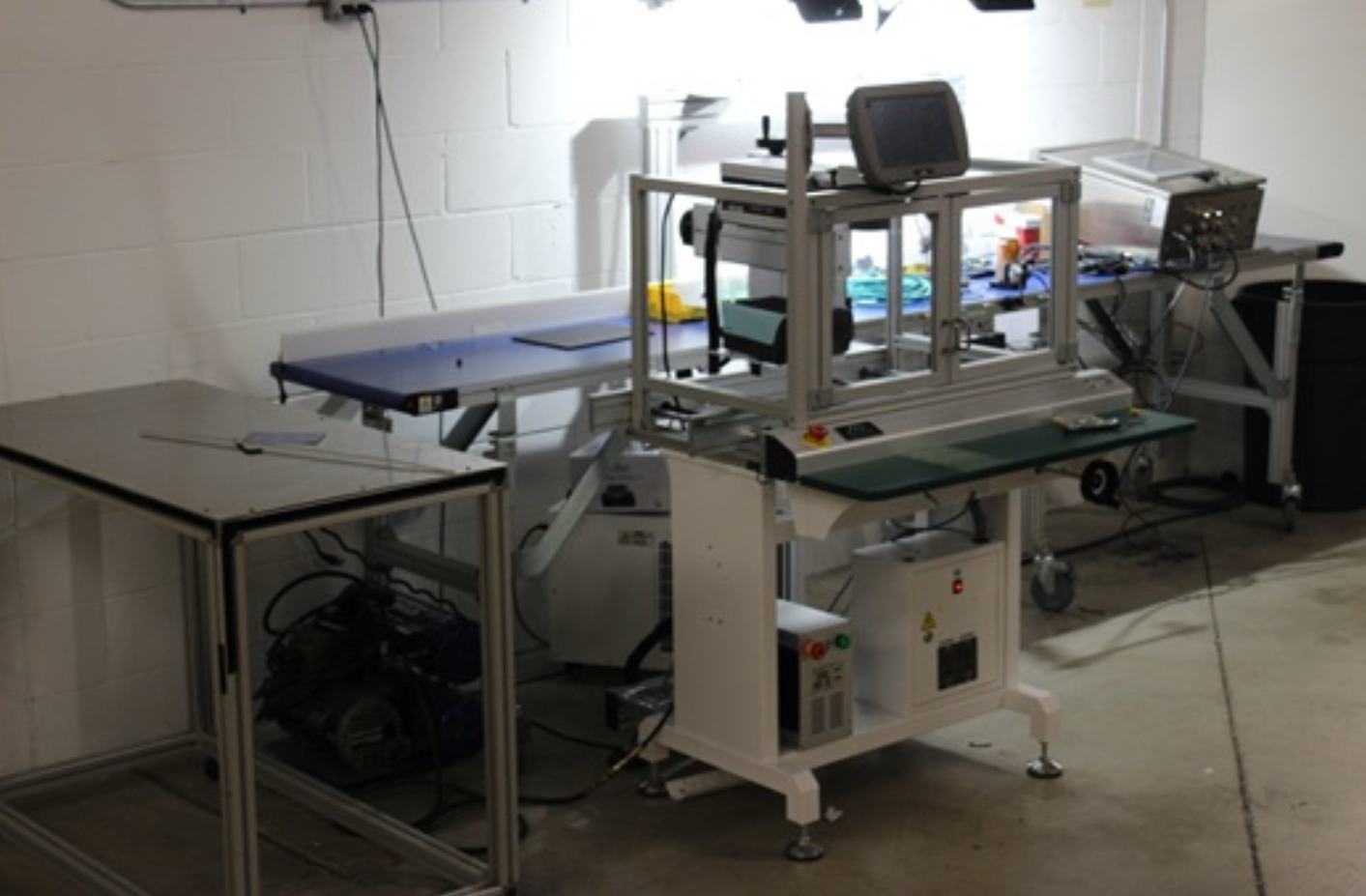
What really sets the Laser Pro apart is its balance of power, precision, and usability. It’s engineered with a high-performance 5W UV laser that delivers detailed marks on delicate materials with near-zero heat affect. But beyond the specs, it’s the system architecture – modular design, advanced motion control, and intuitive software interface – that makes it stand out. It’s not just a laser; it’s a complete solution built for today’s automation-driven factories.
 Could you explain the advantages of UV laser technology in PCB and electronics manufacturing?
UV laser marking operates in a wavelength that interacts more with the surface of the material than penetrating it. This allows for high-contrast, high-resolution marks without damaging the substrate, making it ideal for PCBs, ICs, ceramic substrates, and even transparent or dark plastics. It’s particularly useful for serialization, barcode marking, and traceability in quality-critical environments like aerospace and medical electronics.
In what types of applications or materials does this system particularly excel?
The Laser Pro 5 Watt UV excels in applications involving FR4, ceramics, flex circuits, plastics, and anodized aluminum. It’s also highly effective for marking sensitive medical-grade polymers and coated materials where contrast and edge clarity are critical. Whether it’s a 2D matrix code on a tiny SMT component or lot traceability on a sensor housing, the system delivers uniform, high-quality results.
How does the system ensure precision, repeatability, and minimal thermal impact?
Precision and repeatability are achieved through a combination of high-stability galvanometer scanners, custom-developed motion software, and real-time monitoring systems. The UV wavelength inherently reduces thermal stress, and we further optimize this with pulse control and cooling strategies. We also include closed-loop verification to ensure mark consistency across production runs.
What types of user-friendly features or automation capabilities are built into the Laser Pro?
User-centric design is a big part of our ethos. The Laser Pro includes a touchscreen interface with guided workflows, pre-set material profiles, and real-time diagnostics. From an automation standpoint, it supports full MES integration, barcode validation, and robotic handling interfaces. You can also configure it with inline conveyors or rotary tables depending on your production layout.
Are there specific throughput or performance benchmarks that customers should know about?
Yes. Customers can expect marking cycle times under 2 seconds per PCB in many configurations, depending on content and complexity. Our motion and beam optimization allow for high-speed, high-resolution output without sacrificing mark quality. We also offer customization options for customers with ultra-high-throughput needs.
 What types of companies or industries are seeing the most value from the Laser Pro?
We’re seeing strong adoption in aerospace, medical, and automotive electronics, as well as advanced industrial applications. These sectors have some of the strictest traceability and material handling requirements, which is where the Laser Pro truly shines. Both OEMs and high-mix EMS providers are benefiting from its precision and reliability.
What’s the feedback been like in terms of integration, training, and ongoing support?
Feedback has been overwhelmingly positive. Customers appreciate how easily the system fits into existing workflows, and our support team ensures that integration and training are seamless. We offer both remote and onsite training, and our service model includes preventive maintenance and rapid response. Our software is also designed to be intuitive, which shortens the learning curve significantly.
How do you see UV laser marking evolving in the next few years?
We expect UV laser marking to become more intelligent, connected, and adaptable. AI-driven mark inspection, data-driven process optimization, and even predictive maintenance are on the horizon. As electronics continue to miniaturize and regulatory demands increase, the need for precise, permanent, non-invasive marking will only grow.
Is High-Mark planning any enhancements, accessories, or software developments to complement this system?
Absolutely. We’re actively developing enhanced vision systems for automated mark verification, as well as software modules for traceability data management. We’re also exploring accessories like material handling modules and laser-safe enclosures to help customers deploy the Laser Pro in a broader range of environments.
What’s your vision for where High-Mark technology is headed, and how does the Laser Pro contribute to that vision?
Our vision is to be the trusted partner for intelligent marking solutions in advanced manufacturing. That means developing systems that are not only accurate and robust but also smart and scalable. The Laser Pro embodies that direction, combining high-performance hardware with integration-ready software. It’s more than just a product; it’s a platform that positions our customers – and us – for the future of Industry 4.0.